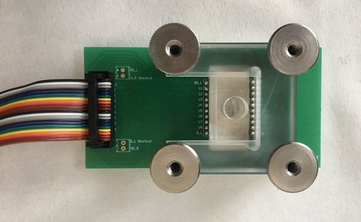
Karthika’s publication, “Fabrication of ITO microelectrodes and electrode arrays using low-cost CO2 laser plotter,” has been recently accepted in Lab on a Chip. The article shows a cost-effective method based on CO2 laser plotter irradiation for preparing ITO microelectrodes. The work was supposed to be a side project but grew and grew till it became a collaboration between our and three more IPC PAS groups.
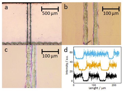
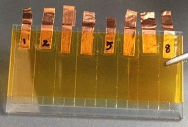
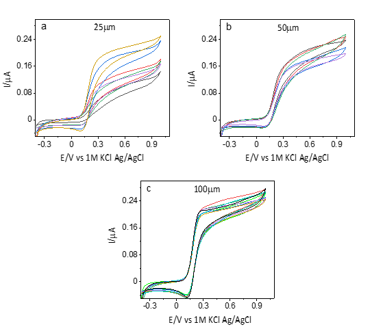
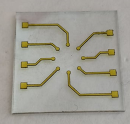
Our CO2 laser, generally used to prepare paper-based electrodes, can also easily ablate ITO layer on glass. Electrodes of different sizes and shapes can be prepared in this manner. At first, rectangular-shaped electrodes were made using direct laser ablation; the smallest sizes optimized were 25, 50, and 100 µm wide.
In a second technique, we engraved patterns onto scotch tape that covered the ITO/glass plates using the CO2 laser. The conducting layer, except the electrodes, was exposed and removed using a solution of FeCl3 and HCl. The cut tape was utilized as a mask to shield the ITO layer on the electrode. This in-situ stencil fabrication followed by etching was the best practice for larger circular-shaped electrodes (diameter 1.75 mm, 2.41 mm2 of geometrical surface area), which were used for impedance evaluation of the state of HepG2 and Hela cell cultures.
Both these methods are efficient and inexpensive means of electrode fabrication.
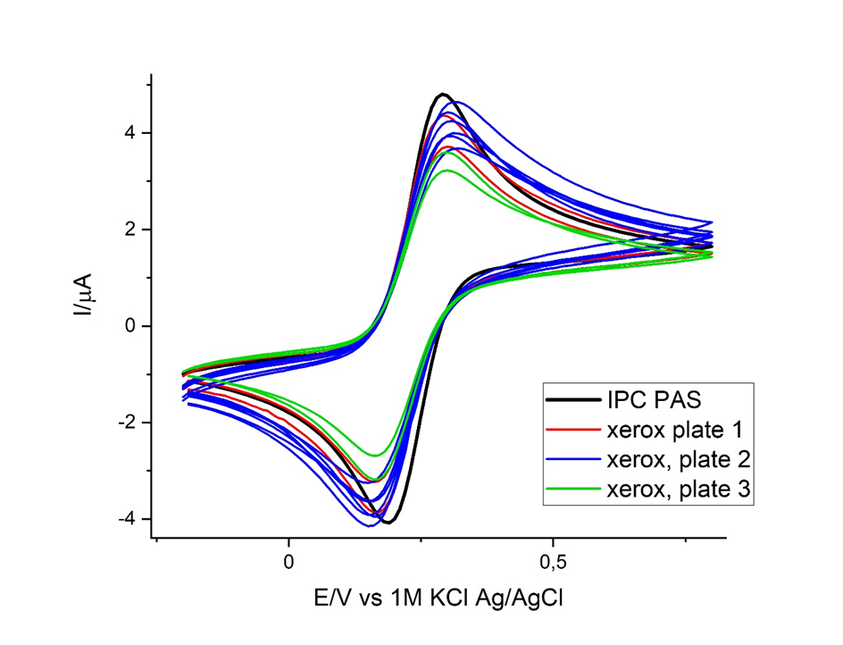
To show that they can be used in resource limited settings, we even went to a local printing shop that had the same equipment and made few batches of electrodes outside the lab!
Even though their reproducibility was a bit lower, they functioned fine. This helped us demonstrate that this technique is practical and can be used even by researchers who don’t have a laser plotter.
Findings from the NCBR LIDER/38/0138/L-9/17/NCBR/2018 project.

1 thought on “Karthika’s article in Lab on a Chip”